
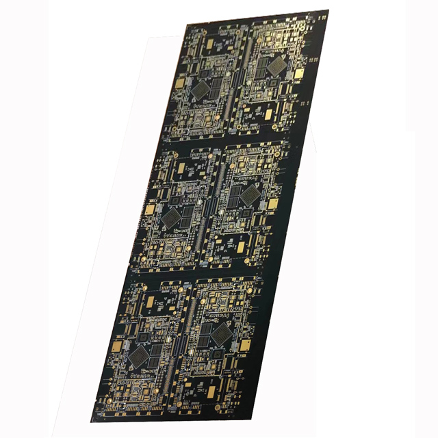
10-Layers Heavy copper PCB
* Layer counts: 10 layers
* Finished board thickness(0.2-6.0mm): 2.0mm
* Base copper thickness: 1 oz
* Finished copper thickness: 4 oz
* Tolerance of the dimension size(±0.1mm)
* Surface Treatment: ENIG
* Impedance Control: Yes
The construction of a heavy copper circuit endows a board with benefits such as:
- Increased endurance to thermal strains.
- Increased current carrying capacity.
- Increased mechanical strength at connector sites and in PTH holes.
- Use of exotic materials to their full potential (i.e., high temperature) without circuit failure.
- Reduced product size by incorporating multiple copper weights on the same layer of circuitry (see Figure 1).
- Heavy copper plated vias carry higher current through the board and help to transfer heat to an external heatsink.
- On-board heatsinks directly plated onto the board surface using up to 120-oz copper planes.
- On-board high-power-density planar transformers
Write your message here and send it to us
-
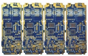
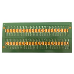
High complexity HDI PCB for industrial product.
-
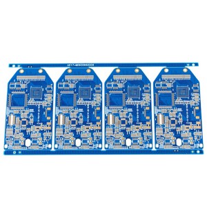
High quality Welldone PCB assembly/PCB Manufact...
-
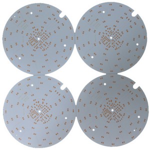
High Quality 3w 9w 12w 18w 90lm/W AC Dob LED Mo...
-
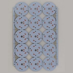
Custom FR4 2835 LED bulb raw material PCB circu...
-
2021 Top Wholesales price Multilayer Rigid-Flex...
-
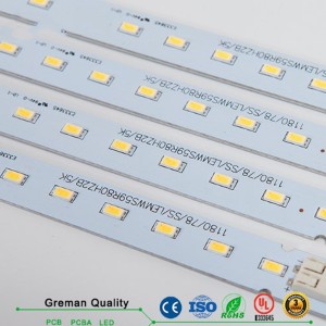
T8 T5 LED light aluminum LED PCB board high lum...