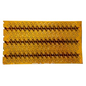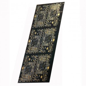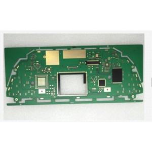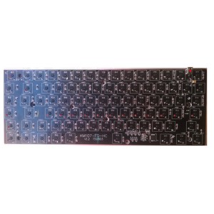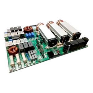
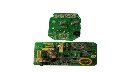


36W PCB With Sensor Ceiling Fan Board
Quick Details:
Type:Rigid PCB
Base Material: FR4 TG140
Copper Thickness:1OZ/2OZ
Board Thickness:1mm
Min. Hole Size:0.01mm
Min. Line Width:0.02mm
Min. Line Spacing:0.01mm
Surface Finishing:HASL
Board Size:Customized
Working temperature:-5℃-60℃
Number of layers:Double Layers
Storage temperature:-20℃-80℃
Rated working voltage:AC100V-250V
Solder mask color:Black.Red.Yellow.White.Blue.Green
PCB Standard:IPC-A-610 E
SMT Efficiency:BGA.QFP.SOP.QFN.PLCC.CHIP
PCB Assembly Test:Visual Inspection (default), AOI, FCT, X-RAY
Substrates Material:Aluminum, 22F,CEM-1,CEM-3,FR4
Breakdown voltage:2.0-2.4KV(AC)
Product Description
Cooperation mode:
1. Schematic design: circuit schematic can be designed according to customer’s requirements.
2, PCB design: PCB diagram can be designed according to the schematic from customer. PCB and bill of materials can be analyzed on the basis of customer’s samples.
3, Software design: SCM software development and design, can be written according to customer’s requirements, with the needed function. Or rewrite some part of software to fit customer’s actual hardware.
Mode of production cooperation:
1. The written program, schematic, PCB data and bill of materials can be sent to customer for the processing of program and circuit boards.
2, We can design the program for customer, help to produce circuit boards according to customer’s requirements. Multi-style cooperation to meet different customer’s needs.
3, Development and design, low charge. only cost and development fees are required, which can be returned after a certain amount of orders. Can be developed and designed on basis of customer’s program requirements.
PCB PROCESSING CAPABILITY :
|
1 |
Layers | Single Sided,2 to 18 Layer |
| 2 | Board material type | FR4,CEM-1,CEM-3,ceramic substrate board,aluminum based board, High-TG, Rogers and more |
| 3 | Compound material lamination | 4 to 6 layers |
| 4 | Maximum dimension | 610 x 1,100mm |
| 5 | Dimension tolerance | ±0.13mm |
| 6 | Board thickness coverage | 0.2 to 6.00mm |
| 7 | Board thickness tolerance | ±10% |
| 8 | DK thickness | 0.076 to 6.00mm |
| 9 | Minimum line width | 0.10mm |
| 10 | Minimum line space | 0.10mm |
| 11 | Outer layer copper thickness | 8.75 to 175µm |
| 12 | Inner layer copper thickness | 17.5 to 175µm |
| 13 | Drilling hole diameter (mechanical drill) | 0.25 to 6.00mm |
| 14 | Finished hole diameter (mechanical drill) | 0.20 to 6.00mm |
| 15 | Hole diameter tolerance (mechanical drill) | 0.05mm |
| 16 | Hole position tolerance (mechanical drill) | 0.075mm |
| 17 | Laser drill hole size | 0.10mm |
| 18 | Board thickness and hole diameter ratio | 10:1 |
| 19 | Solder mask type | Green, Yellow, Black, Purple, Blue, White and Red |
| 20 | Minimum solder mask | Ø0.10mm |
| 21 | Minimum size of solder mask separation ring | 0.05mm |
| 22 | Solder mask oil plug hole diameter | 0.25 to 0.60mm |
| 23 | Impedance control tolerance | ±10% |
| 24 | Surface finish | Hot air level, ENIG, immersion silver, gold plating, immersion tin and gold finger |