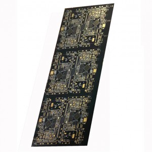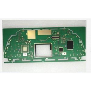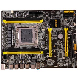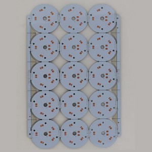
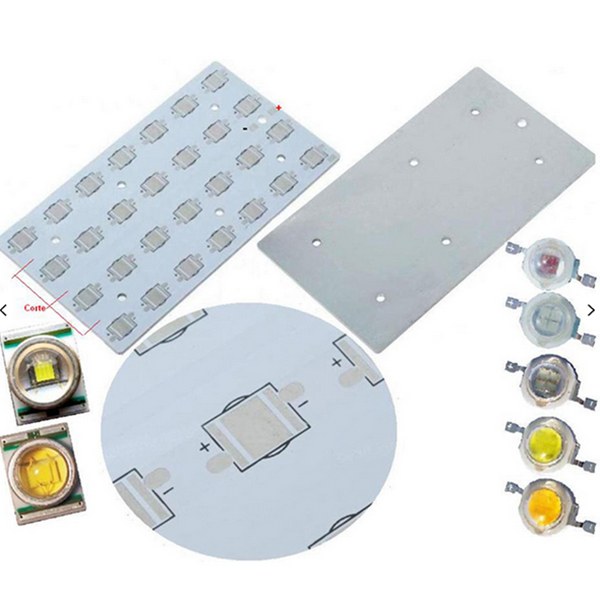


High Power LED Traffic Light PCB and Electronic Components Stores
Product Details
Base Material: FR-4, FR2.Taconic, Rogers
Copper Thickness: 1/2 oz min; 12 oz max
Board Thickness: 0.2mm-6.00 mm(8mil-126mil)
Min. Hole Size: 0.1mm(4mil)
Min. Line Width: 0.075mm(3mil)
Min. Line Spacing: 0.1mm4mil)
Surface Finishing: Immersion Gold/Au, HASL, OSP, etc.
Warp & Twist: 0.7%
Hole Position: +/-0.075mm(3mil) CNC Drilling
Insulation Resistance: 10Kohm-20Mohm
Conductivity: <50ohm
Test Voltage: 10-300V
ANCE Control: +/-10%
Different Impenitence: +-/10%
Outline Tolerance: +/-0.125mm(5mil) CNC Routing +/-0.15mm(6mil) by Punching
Hole Diameter(H) PTH L: +/-0.075mm(3mil) NON-PTH L: +/-0.05mm(2mil)
Conductor Width(W): +/-20% of original artwork PTH L: +/-0.
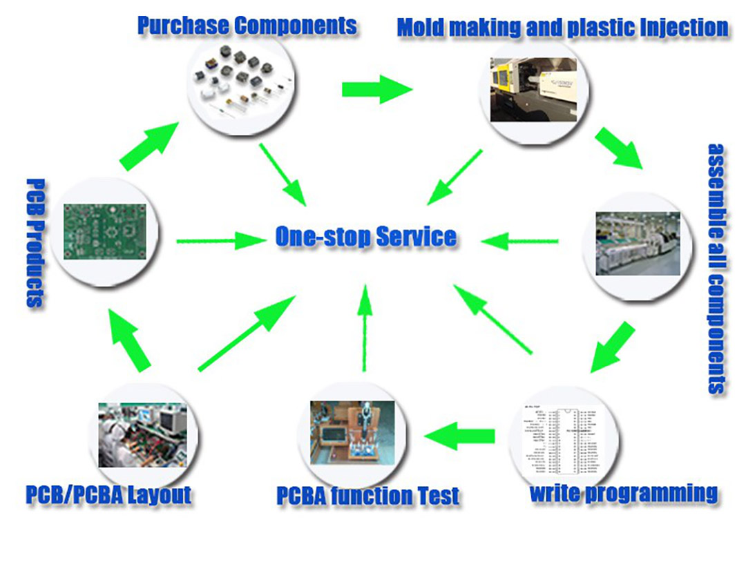
Our Services
We can provide one-stop service:
1. PCB circuit boards.
2. E-test.
3.Electronic components purchasing.
4. PCB assembly: available on SMT, BGA, DIP.
5. PCBA function test.
6. Enclosure assembly.
PCB product Capacity
| PCB Manufacture Capacity | |
| Item | Specification |
| Material | FR-4, FR1,FR2; CEM-1, CEM-3,Rogers, Teflon,Arlon,Aluminum Base, Copper Base,Ceramic, Crockery, etc. |
| Remarks | High Tg CCL is Available(Tg>=170℃) |
| Finish Board Thickness | 0.2 mm-6.00mm(8mil-126mil) |
| Surface Finish | Gold finger(>=0.13um), Immersion Gold(0.025-0075um), Plating Gold(0.025-3.0um), HASL(5-20um), OSP(0.2-0.5um) |
| Shape | Routing,Punch,V-cut,Chamfer |
| Surface Treatment | Solder Mask(black, green, white, red, blue, thickness>=12um, Block, BGA) |
| Silkscreen(black, yellow, white) | |
| Peel able-mask(red, blue, thickness>=300um) | |
| Minimum Core | 0.075mm(3mil) |
| Copper Thickness | 1/2 oz min; 12oz max |
| Min Trace Width & Line Spacing | 0.075mm/0.075mm(3mil/3mil) |
| Min Hole Diameter for CNC Drilling | 0.1mm(4mil) |
| Min Hole Diameter for Punching | 0.6mm(35mil) |
| Biggest panel size | 610mm * 508mm |
| Hole Position | +/-0.075mm(3mil) CNC Drilling |
| Conductor Width(W) | +/-0.05mm(2mil) or +/-20% of original |
| Hole Diameter(H) | PTHL:+/-0.075mm(3mil) |
| Non PTHL:+/-0.05mm(2mil) | |
| Outline Tolerance | +/-0.1mm(4mil) CNC Routing |
| Warp & Twist | 0.70% |
| Insulation Resistance | 10Kohm-20Mohm |
| Conductivity | <50ohm |
| Test Voltage | 10-300V |
| Panel Size | 110 x 100mm(min) |
| 660 x 600mm(max) | |
| Layer-layer misrepresentation | 4 layers:0.15mm(6mil)max |
| 6 layers:0.25mm(10mil)max | |
| Min spacing between hole edge to circuitry pattern of an inner layer | 0.25mm(10mil) |
| Min spacing between board outline to circuitry pattern of an inner layer | 0.25mm(10mil) |
| Board thickness tolerance | 4 layers:+/-0.13mm(5mil) |