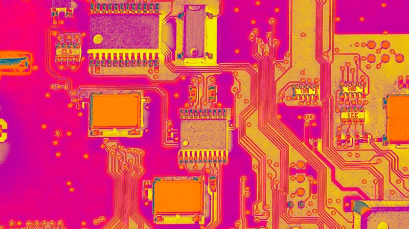
Thanks to the recent rise of affordable circuit board production services, many people reading Hackaday are just now learning the art of PCB design. For those of you still producing the “Hello World” equivalent of FR4, all traces are getting where they’re supposed to be, and that’s enough. But eventually, your designs will become more ambitious, and with this added complexity will naturally come new design considerations. For example, how to prevent the PCB from burning itself out in high current applications?
That’s exactly the question Mike Jouppi wanted to help answer when he hosted the Hack Chat last week. It’s a topic he takes so seriously that he started a company called Thermal Management LLC dedicated to helping engineers with PCB thermal design. He also chaired the development of IPC-2152, a standard for properly sizing circuit board traces based on the amount of current the board needs to carry. This is not the first standard to address the issue, but it is certainly the most modern and comprehensive.
For many designers, it is common for them to refer to data dating back to the 1950s in some cases, simply out of prudence to increase their traces. Often this is based on concepts that Mike says his research has found inaccurate, such as assuming that the internal traces of a PCB tend to be hotter than the external traces. The new standard is designed to help designers avoid these potential pitfalls, although he points out that it is still an imperfect simulation of the real world; additional data such as mounting configuration needs to be considered to better understand the thermal characteristics of the board.
Even with such a complex subject, there are some broadly applicable tips to keep in mind. Substrates always have poor thermal performance compared to copper, so using internal copper planes can help conduct heat through the board, Mike said. When dealing with SMD parts that generate a lot of heat, large copper-plated vias can be used to create parallel thermal paths.
Towards the end of the chat, Thomas Shaddack had an interesting thought: Since the resistance of traces increases with temperature, can this be used to determine the temperature of otherwise hard-to-measure internal PCB traces? Mike says the concept is sound, but if you want to get accurate readings, you need to know the nominal resistance of the trace you are calibrating. Something to keep in mind going forward, especially if you don’t have a thermal camera that lets you peek into the inner layers of your PCB.
While hacker chats are usually informal, this time we noticed some pretty poignant issues. Some people have very specific problems and need some help. It can be difficult to resolve all the nuances of complex issues in a public chat, so in some cases, we know that Mike is connecting directly with attendees so that he can discuss issues with them one-on-one.
While we can’t always guarantee that you’ll get that kind of personalized service, we think it’s a testament to the unique networking opportunities available to those who participate in Hack Chat and thank Mike for going the extra mile to make sure everyone’s answering the best he can problem.
Hack Chat is a weekly online chat session hosted by leading experts from all corners of the hardware hacking field. It’s a fun and informal way to get in touch with hackers, but if you can’t make it, these overview posts and transcripts posted to Hackaday.io make sure you don’t miss out.
So the physics of the 1950s still apply, but if you use a lot of layers, and inject a lot of copper in between, the inner layers may not be more insulating.
Post time: Apr-22-2022

