100% Original Relay Pcb Design - Multilayer PCB Schematic Design Fabrication Services Custom Design 2 Layer LED PCB Printed Circuit Boards – Welldone
100% Original Relay Pcb Design - Multilayer PCB Schematic Design Fabrication Services Custom Design 2 Layer LED PCB Printed Circuit Boards – Welldone Detail:
Product Details
Base Material:FR4/ Aluminum/ Ceramic/ PI
Copper Thickness:3oz
Board Thickness:2.0mm
Min. Hole Size:4mil
Min. Line Width:4mil
Min. Line Spacing:4mil
Surface Finishing:HASL
Product name:Multilayer PCB Custom Design 2 Layer LED PCB Printed Circuit Boards
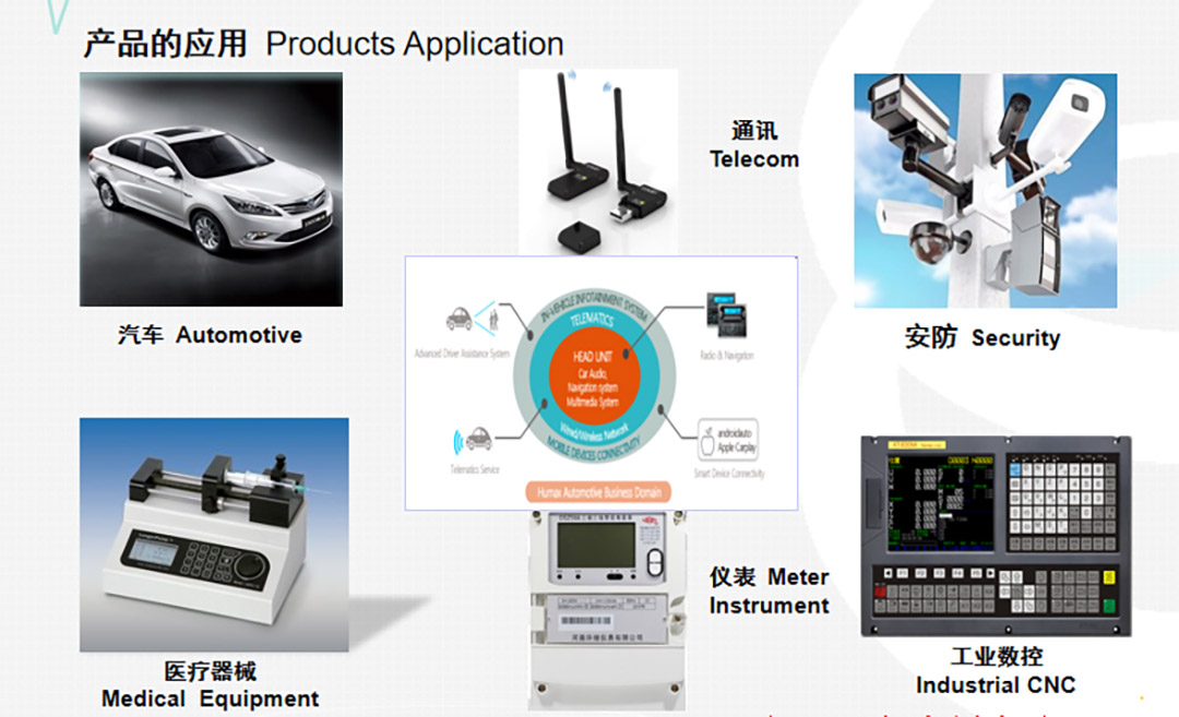
Application:Electronics Device
Type:Electronic Board
Certificate:ROSH. ISO9001. UL. ISO13485
Usage:OEM Electronics
Item:ODM OEM LED PCBA
Name:PCB Board Production
Solder mask:Green. Red. Blue. White. Black.Yellow
Material:FR4 /aluminum/ceramic
Service:One-stop Turnkey Service
| Item | Normal capacity | Limit capacity | Item | Normal capacity | Limit capacity |
| Layer No. | 2-16 | ≤20 | Max. copper thickness( Inner layer) | 4OZ | 5OZ |
| Core board thickness | 0.075-2.0mm | 0.05-3.0mm | Max. copper thickness( Outer layer) | 4OZ | 6OZ |
| min. PTH to copper | 165.1um | 152.4um | Min. space between SMD pads for S/M bridge | 203.2um | 177.8um |
| Board thickness(double sides) | 0.3-3.2mm | 0.3-4mm | Minimum legend width/height | 127um /762um | 101.6um /609.6um |
| Board thickness(Multi-layer) | 0.6-3.2mm | 0.6-4mm | Outline dimension tolerance | ±101.6um | ±76.2um |
| Tolerance of board thickness(T≤0.8mm) | 0.1mm | 0.075mm | Bow & twist (T≤1mm) | ≤0.75% | ≤0.5% |
| Tolerance of board thickness(T>0.8mm) | ±10% | ±5% | Bow & twist (T≤1mm) | ≤0.5% | ≤0.3% |
| Min. line width | 76.2um | 63.5um | Precision of hole to hole | ±0.05mm | / |
| Minimum line space | 68.58um | 63.5um | Impedance control range | ±10% | ±8% |
| Minimum hole diameter | 0.2mm | 0.15mm | Aspect ratio (0.2mm) | 10:1 | 12:1 |
| Tolerance of press fit hole diameter | 0.05mm | 0.05mm | Finished product size | 55-600mm | 10-620mm |
| profiling method | CNC、 V-CUT、 Punching or mold | ||||
| Surface treatment | EING、 OSP、 Immersion silver、 Selective OSP+ENIG | ||||
| Laminate type | FR-4.0, FR-4.1(Normal TG, middle TG, high TG), CEM-3, | ||||
Q1:Are you a factory or trade company?
A: Yes, we are the factory, we have our own PCB manufacturing & Assembly factory.
Q2:What kind of PCB file format can you accept for production?
A:Gerber, PROTEL 99SE, PROTEL DXP, POWER PCB, CAM350, GCCAM, ODB+(.TGZ)
Q3:Are my PCB files safe when I submit them to you for manufacturing?
A:We respect customer’s copyright and will never manufacture PCB for someone else with your files unless we receive written. Permission from you, nor we’ll share these files with any other 3rd parties.
Q4:No PCB file/GBR file, only have the PCB sample,can you produce it for me?
A: Yes,we could help you to clone the PCB. Just send the sample PCB to us, we could clone the PCB design and work out it.
Q5:What is the lead time?
A:Sample:
1-2 Layers: 5 to 7working days
4-8 Layers: 12 working days
Mass production:
1-2 Layers:7 to 15 working days
4-8 Layers:10 to 18 working days
The lead time is depends on your final confirmed quantity.
Q6:What payment do you accept ?
A:-Wire Transfer(T/T)
-Western Union
-Letter of Credit(L/C)
-Paypal
-Ali Pay
-Credit Cart
Q7:How to get the PCBS?
A:For small packages, we will ship the boards to you by DHL,UPS,FedEx,EMS. Door to door service! You will get your PCBS at your home.
For heavy goods more than 300kg, we may ship your PC boards by ship or by air to save freight cost. Of course, if you have your own forwarder, we may contact them for dealing with your shipment.
Q8:What is your minimum order quantity?
A: No MOQ.
Q9:How about your factory production capacity?
A:we can provide 100000 square meter/month.
Q10:Which countries have you worked with?
A:US, Canada, Italy, Germany, Czech Republic, Australia, Japan, and so on.
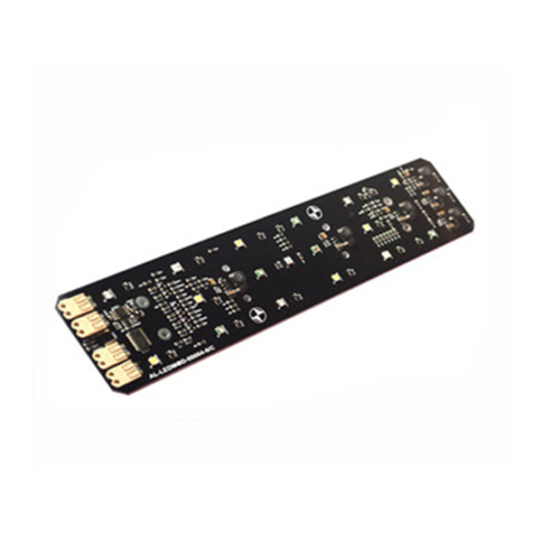
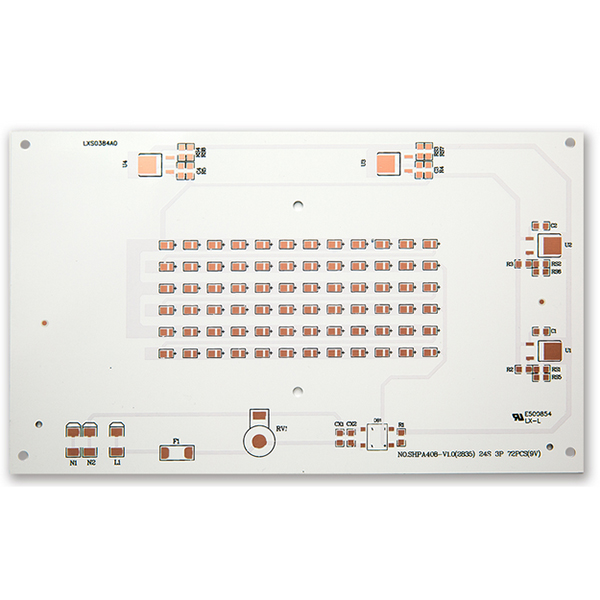
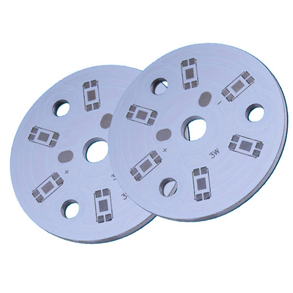
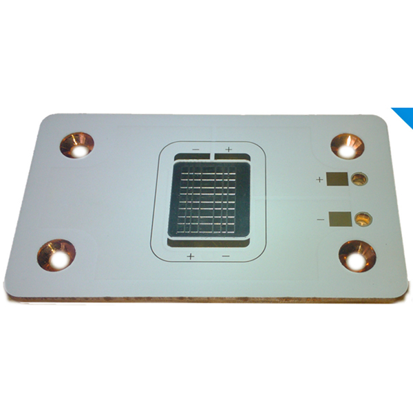
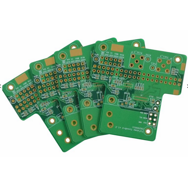
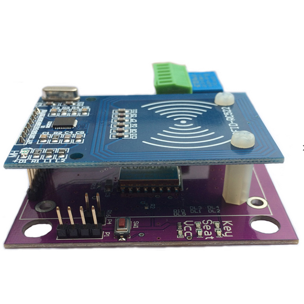
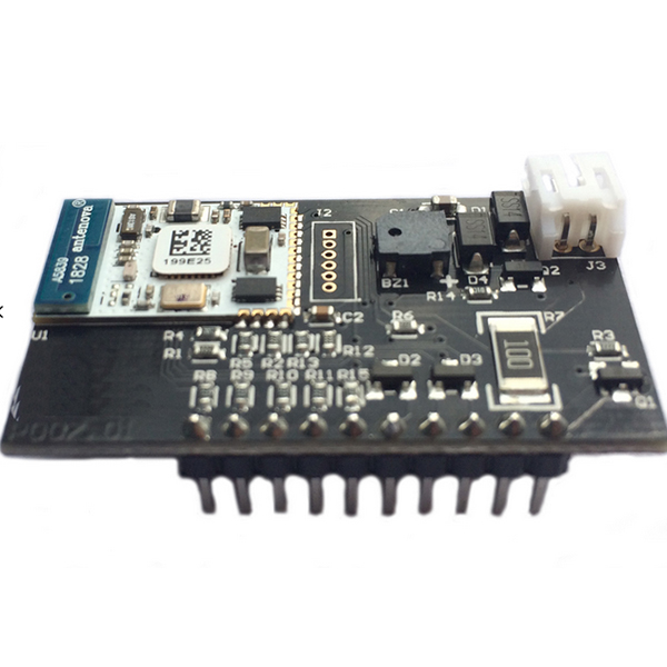
Product detail pictures:

Related Product Guide:
Gaining purchaser gratification is our firm's intention eternally. We will make wonderful endeavours to build new and top-quality merchandise, satisfy your exclusive needs and provide you with pre-sale, on-sale and after-sale products and services for 100% Original Relay Pcb Design - Multilayer PCB Schematic Design Fabrication Services Custom Design 2 Layer LED PCB Printed Circuit Boards – Welldone , The product will supply to all over the world, such as: USA, Paraguay, South Africa, Upon today, we have customers from all over the world, including USA, Russia, Spain, Italy, Singapore, Malaysia, Thailand, Poland, Iran and Iraq. The mission of our company is to provide the highest quality products with best price. We are looking forward to doing business with you.
With a positive attitude of "regard the market, regard the custom, regard the science", the company works actively to do research and development. Hope we have a future business relationships and achieving mutual success.