Factory Free sample Pcb Case Design - EMC Design Spark FR4 PCB And The Printed Circuit Board – Welldone
Factory Free sample Pcb Case Design - EMC Design Spark FR4 PCB And The Printed Circuit Board – Welldone Detail:
Product Details
Base Material:FR4
Copper Thickness:1oz
Board Thickness:1.6mm
Min. Hole Size:0.2mm
Min. Line Width:0.1mm
Min. Line Spacing:0.1mm
Surface Finishing:HASL
Solder Mask:Green
Silkscreen:White
PCB Test:Test-rig,Flying Probe Test
PCBA Test:X-ray,AOI Test,Functional test
Certificate:UL. ROHS. CE
Type of services:High Quality PCB Manufacturing
Keywords:blank PCB board price
Service:One-stop Service
Layer:1-24layers
|
Item |
Specification |
|
|
1 |
Number of Layer |
1-18Layers |
|
2 |
Material |
FR-4,FR2.Ta-conic,Rogers, CEM-1 CEM-3,ceramic , crockery Metal-backed Laminate |
| 3 |
Surface Finish |
HASL(LF), Gold plating, Electrolysis nickel immersion gold, Immersion Tin, OSP |
|
4 |
Finish Board Thickness |
0.2mm-6.00 mm(8mil-126mil) |
|
5 |
Copper Thickness |
1/2 oz min;12 oz max |
|
6 |
Solder Mask |
Green/Black/White/Red/Blue/Yellow |
|
7 |
Min.Trace Width & Line Spacing |
0.075mm/0.1mm(3mil/4mil) |
|
8 |
Min.Hole Diameter for CNC Drilling |
0.1mm(4mil) |
|
9 |
Min.Hole Diameter for punching |
0.9mm(35mil) |
|
10 |
Biggest panel size |
610mm*508mm |
|
11 |
Hole Position |
+/-0.075mm(3mil) CNC Drilling |
|
12 |
Conductor Width(W) |
0.05mm(2mil)or; +/-20% of original artwork |
|
13 |
Hole Diameter(H) |
PTH L:+/-0.075mm(3mil); NON-PTH L:+/-0.05mm(2mil) |
|
14 |
Outline Tolerance |
0.125mm(5mil) CNC Routing; +/-0.15mm(6mil) by Punching |
|
15 |
Warp & Twist |
0.70% |
|
16 |
Insulation Resistance |
10Kohm-20Mohm |
|
17 |
Conductivity |
<50ohm |
|
18 |
Test Voltage |
10-300V |
|
19 |
Panel Size |
110×100mm(min);660×600mm(max) |
|
20 |
Layer-layer ministration |
4 layers:0.15mm(6mil)max; 6 layers:0.25mm(10mil)max |
|
21 |
Min.spacing between hole edge to circuity pattern of an inner layer |
0.25mm(10mil) |
|
22 |
Min.spacing between board outline circuitry pattern of an inner layer |
0.25mm(10mil) |
|
23 |
Board thickness tolerance |
4 layers:+/-0.13mm(5mil); 6 layers:+/-0.15mm(6mil) |
|
24 |
Impedance Control |
+/-10% |
|
25 |
Different Impedance |
+-/10% |
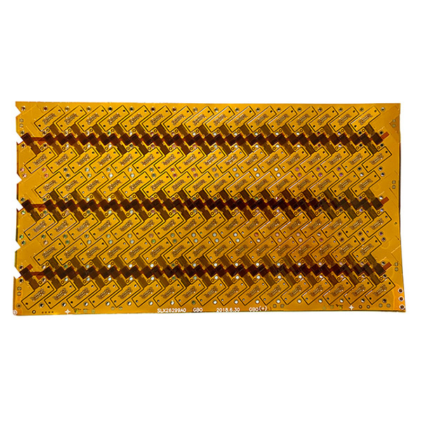
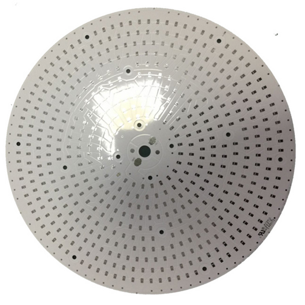
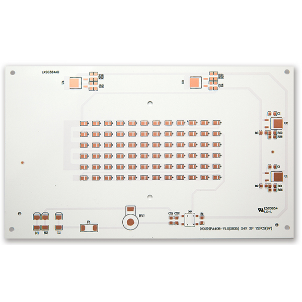
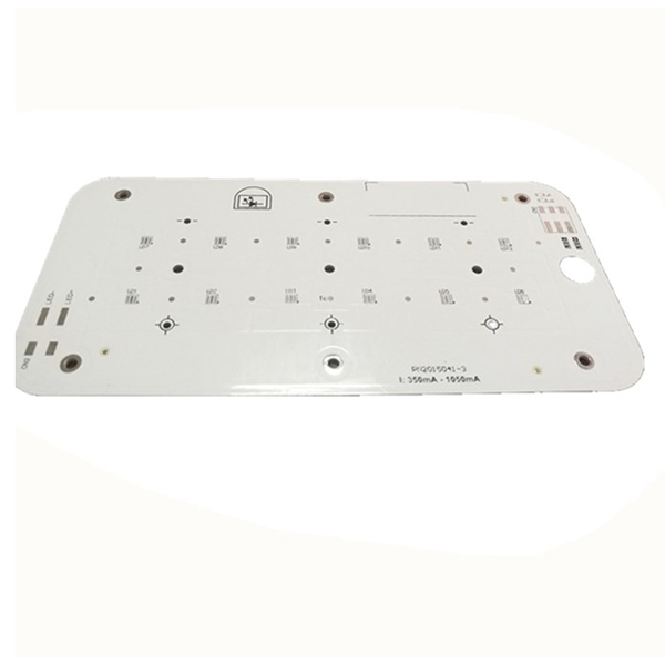
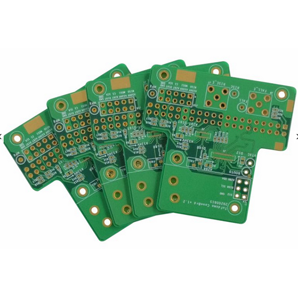
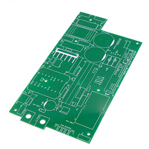
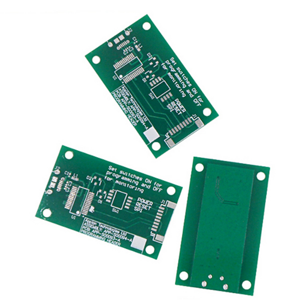
Product detail pictures:
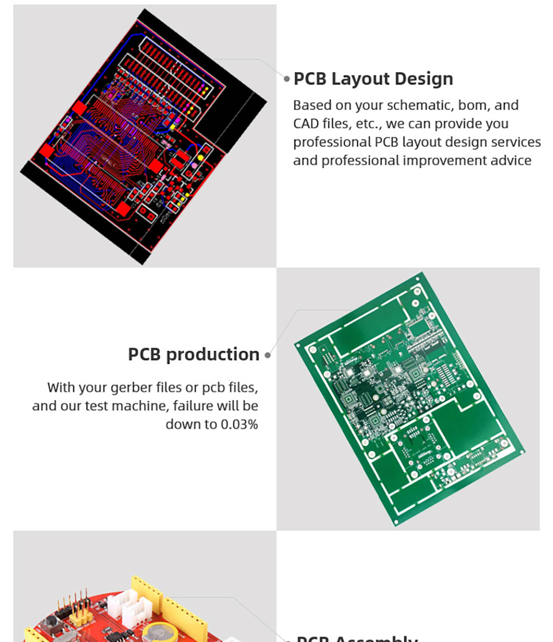
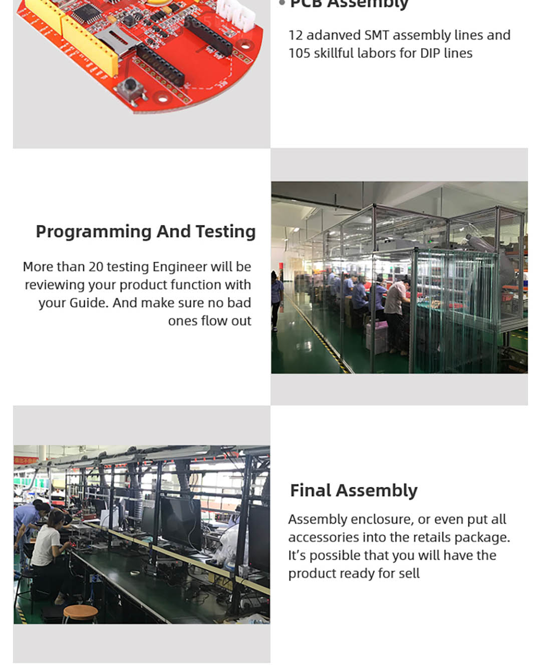
Related Product Guide:
With this motto in mind, we've turn into one of quite possibly the most technologically innovative, cost-efficient, and price-competitive manufacturers for Factory Free sample Pcb Case Design - EMC Design Spark FR4 PCB And The Printed Circuit Board – Welldone , The product will supply to all over the world, such as: Albania, Liberia, Turkey, Taking the core concept of "to be the Responsible". We'll redound up on society for high quality merchandise and good service. We will initiative to participate in international competition to be a first- class manufacturer of this product in the world.
The supplier cooperation attitude is very good, encountered various problems, always willing to cooperate with us, to us as the real God.