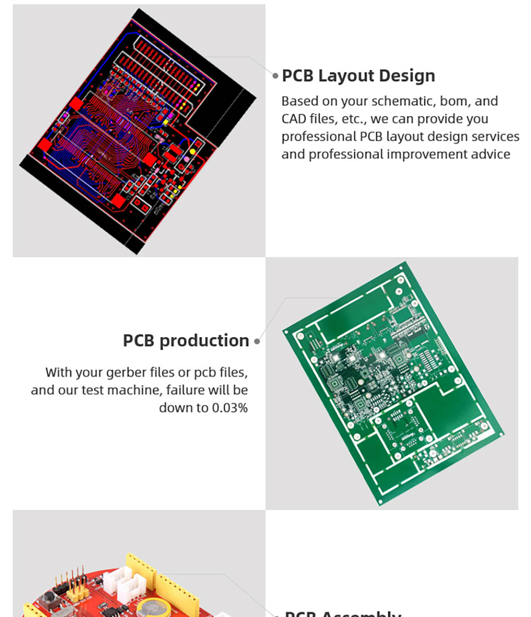
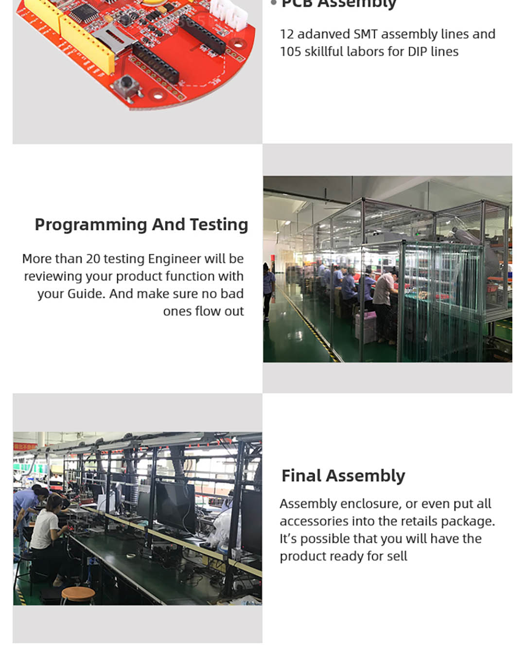
OEM Customized Double Layer Pcb Design - EMC Design Spark FR4 PCB And The Printed Circuit Board – Welldone
OEM Customized Double Layer Pcb Design - EMC Design Spark FR4 PCB And The Printed Circuit Board – Welldone Detail:
Product Details
Base Material:FR4
Copper Thickness:1oz
Board Thickness:1.6mm
Min. Hole Size:0.2mm
Min. Line Width:0.1mm
Min. Line Spacing:0.1mm
Surface Finishing:HASL
Solder Mask:Green
Silkscreen:White
PCB Test:Test-rig,Flying Probe Test
PCBA Test:X-ray,AOI Test,Functional test
Certificate:UL. ROHS. CE
Type of services:High Quality PCB Manufacturing
Keywords:blank PCB board price
Service:One-stop Service
Layer:1-24layers
|
Item |
Specification |
|
|
1 |
Number of Layer |
1-18Layers |
|
2 |
Material |
FR-4,FR2.Ta-conic,Rogers, CEM-1 CEM-3,ceramic , crockery Metal-backed Laminate |
| 3 |
Surface Finish |
HASL(LF), Gold plating, Electrolysis nickel immersion gold, Immersion Tin, OSP |
|
4 |
Finish Board Thickness |
0.2mm-6.00 mm(8mil-126mil) |
|
5 |
Copper Thickness |
1/2 oz min;12 oz max |
|
6 |
Solder Mask |
Green/Black/White/Red/Blue/Yellow |
|
7 |
Min.Trace Width & Line Spacing |
0.075mm/0.1mm(3mil/4mil) |
|
8 |
Min.Hole Diameter for CNC Drilling |
0.1mm(4mil) |
|
9 |
Min.Hole Diameter for punching |
0.9mm(35mil) |
|
10 |
Biggest panel size |
610mm*508mm |
|
11 |
Hole Position |
+/-0.075mm(3mil) CNC Drilling |
|
12 |
Conductor Width(W) |
0.05mm(2mil)or; +/-20% of original artwork |
|
13 |
Hole Diameter(H) |
PTH L:+/-0.075mm(3mil); NON-PTH L:+/-0.05mm(2mil) |
|
14 |
Outline Tolerance |
0.125mm(5mil) CNC Routing; +/-0.15mm(6mil) by Punching |
|
15 |
Warp & Twist |
0.70% |
|
16 |
Insulation Resistance |
10Kohm-20Mohm |
|
17 |
Conductivity |
<50ohm |
|
18 |
Test Voltage |
10-300V |
|
19 |
Panel Size |
110×100mm(min);660×600mm(max) |
|
20 |
Layer-layer ministration |
4 layers:0.15mm(6mil)max; 6 layers:0.25mm(10mil)max |
|
21 |
Min.spacing between hole edge to circuity pattern of an inner layer |
0.25mm(10mil) |
|
22 |
Min.spacing between board outline circuitry pattern of an inner layer |
0.25mm(10mil) |
|
23 |
Board thickness tolerance |
4 layers:+/-0.13mm(5mil); 6 layers:+/-0.15mm(6mil) |
|
24 |
Impedance Control |
+/-10% |
|
25 |
Different Impedance |
+-/10% |
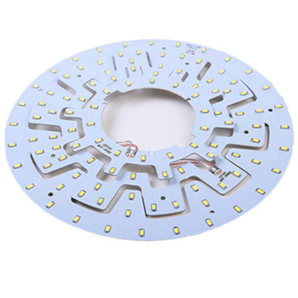
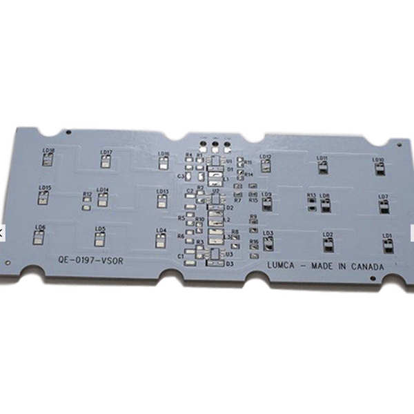
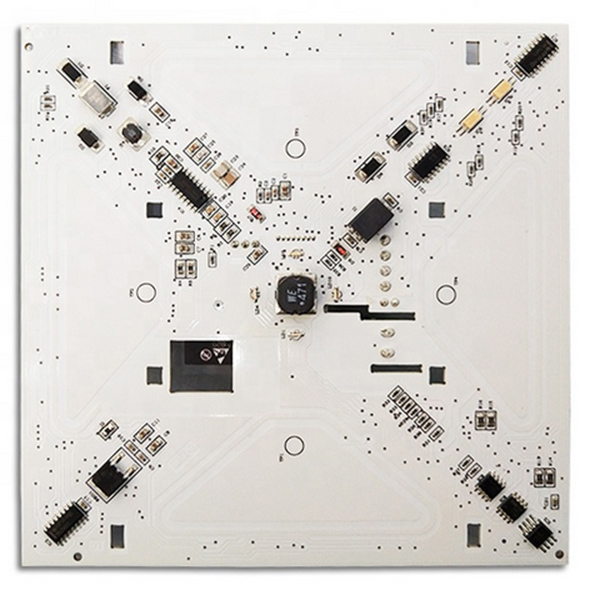
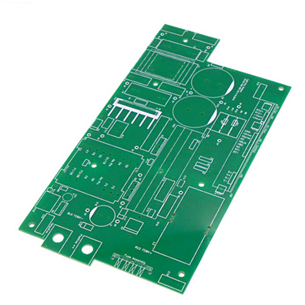
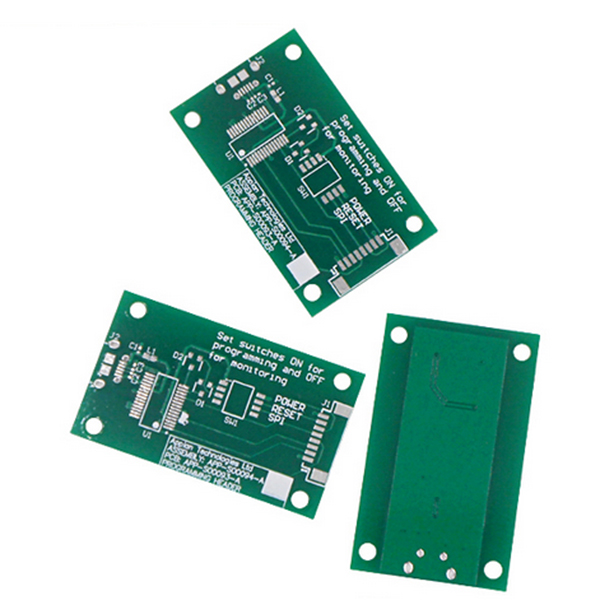
Product detail pictures:
Related Product Guide:
Our commission should be to provide our end users and clients with very best excellent and aggressive portable digital products and solutions for OEM Customized Double Layer Pcb Design - EMC Design Spark FR4 PCB And The Printed Circuit Board – Welldone , The product will supply to all over the world, such as: Curacao, Cyprus, Lebanon, Based on our guiding principle of quality is the key to development, we continually strive to exceed our customers' expectations. As such, we sincerely invite all interested companies to contact us for future cooperation, We welcome old and new customers to hold hands together for exploring and developing; For more information, be sure to feel free to contact us. Thanks. Advanced equipment, strict quality control, customer-orientation service, initiative summary and improvement of defects and extensive industry experience enable us to guarantee more customer satisfaction and reputation which, in return, brings us more orders and benefits. If you are interested in any of our merchandise, make sure you feel free to contact us. Inquiry or visit to our company are warmly welcome. We sincerely hope to start a win-win and friendly partnership with you. You can see more details in our website.
Good quality, reasonable prices, rich variety and perfect after-sales service, it's nice!