
OEM Customized Double Layer Pcb Design - EMC Design Spark FR4 PCB And The Printed Circuit Board – Welldone
OEM Customized Double Layer Pcb Design - EMC Design Spark FR4 PCB And The Printed Circuit Board – Welldone Detail:
Product Details
Base Material:FR4
Copper Thickness:1oz
Board Thickness:1.6mm
Min. Hole Size:0.2mm
Min. Line Width:0.1mm
Min. Line Spacing:0.1mm
Surface Finishing:HASL
Solder Mask:Green
Silkscreen:White
PCB Test:Test-rig,Flying Probe Test
PCBA Test:X-ray,AOI Test,Functional test
Certificate:UL. ROHS. CE
Type of services:High Quality PCB Manufacturing
Keywords:blank PCB board price
Service:One-stop Service
Layer:1-24layers
|
Item |
Specification |
|
|
1 |
Number of Layer |
1-18Layers |
|
2 |
Material |
FR-4,FR2.Ta-conic,Rogers, CEM-1 CEM-3,ceramic , crockery Metal-backed Laminate |
| 3 |
Surface Finish |
HASL(LF), Gold plating, Electrolysis nickel immersion gold, Immersion Tin, OSP |
|
4 |
Finish Board Thickness |
0.2mm-6.00 mm(8mil-126mil) |
|
5 |
Copper Thickness |
1/2 oz min;12 oz max |
|
6 |
Solder Mask |
Green/Black/White/Red/Blue/Yellow |
|
7 |
Min.Trace Width & Line Spacing |
0.075mm/0.1mm(3mil/4mil) |
|
8 |
Min.Hole Diameter for CNC Drilling |
0.1mm(4mil) |
|
9 |
Min.Hole Diameter for punching |
0.9mm(35mil) |
|
10 |
Biggest panel size |
610mm*508mm |
|
11 |
Hole Position |
+/-0.075mm(3mil) CNC Drilling |
|
12 |
Conductor Width(W) |
0.05mm(2mil)or; +/-20% of original artwork |
|
13 |
Hole Diameter(H) |
PTH L:+/-0.075mm(3mil); NON-PTH L:+/-0.05mm(2mil) |
|
14 |
Outline Tolerance |
0.125mm(5mil) CNC Routing; +/-0.15mm(6mil) by Punching |
|
15 |
Warp & Twist |
0.70% |
|
16 |
Insulation Resistance |
10Kohm-20Mohm |
|
17 |
Conductivity |
<50ohm |
|
18 |
Test Voltage |
10-300V |
|
19 |
Panel Size |
110×100mm(min);660×600mm(max) |
|
20 |
Layer-layer ministration |
4 layers:0.15mm(6mil)max; 6 layers:0.25mm(10mil)max |
|
21 |
Min.spacing between hole edge to circuity pattern of an inner layer |
0.25mm(10mil) |
|
22 |
Min.spacing between board outline circuitry pattern of an inner layer |
0.25mm(10mil) |
|
23 |
Board thickness tolerance |
4 layers:+/-0.13mm(5mil); 6 layers:+/-0.15mm(6mil) |
|
24 |
Impedance Control |
+/-10% |
|
25 |
Different Impedance |
+-/10% |
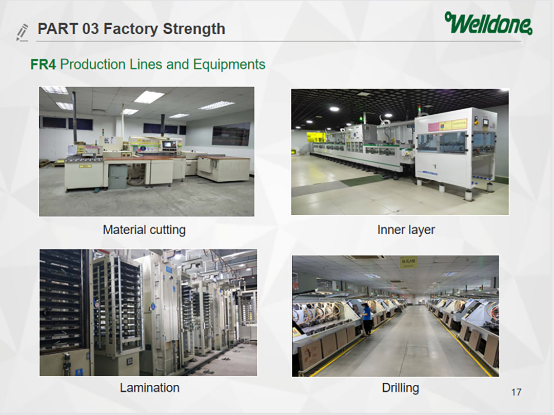
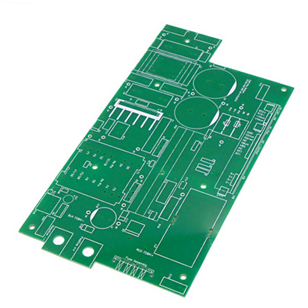
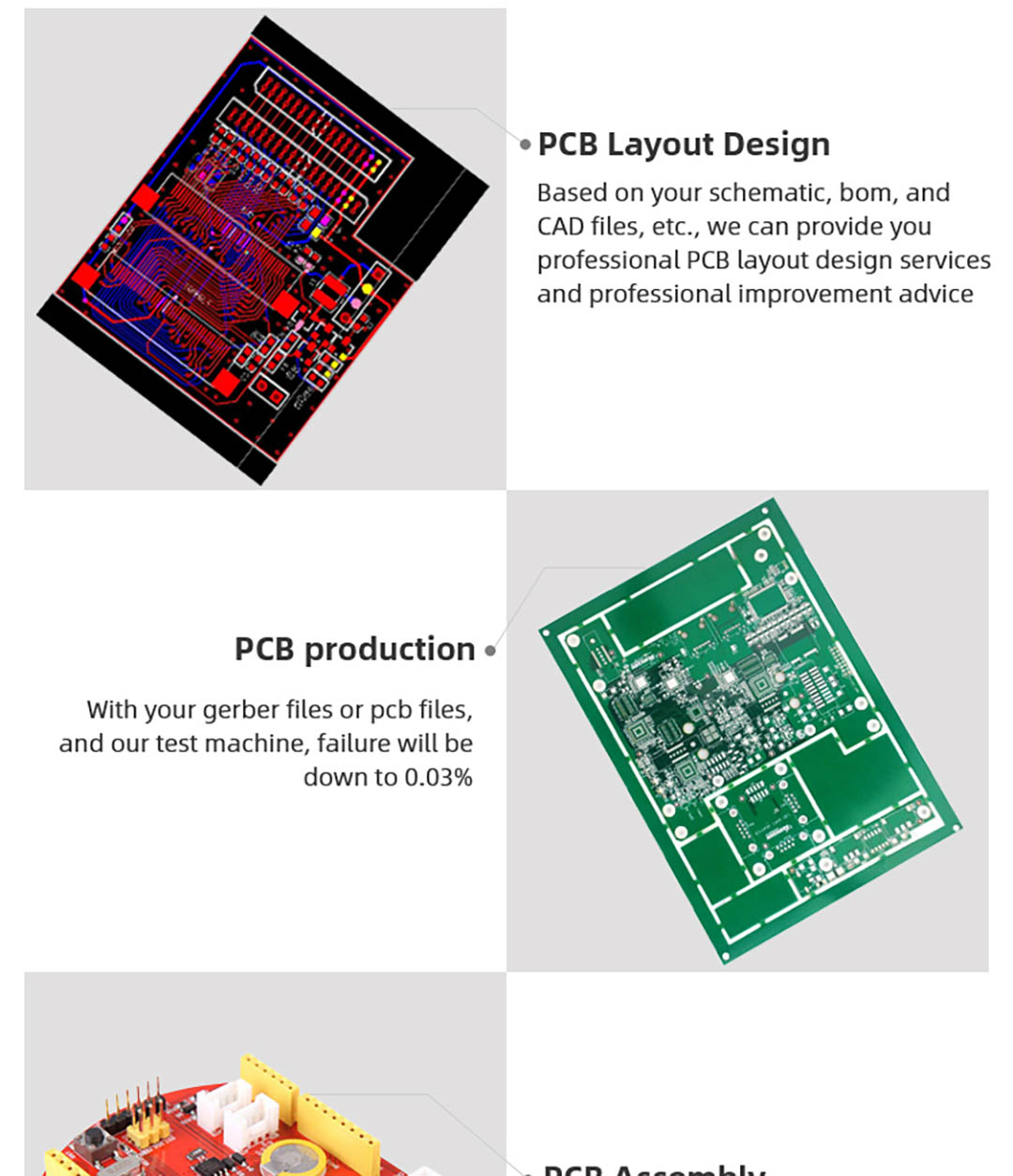
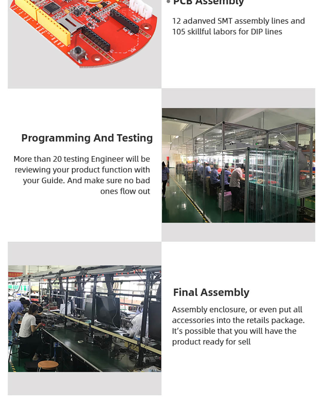
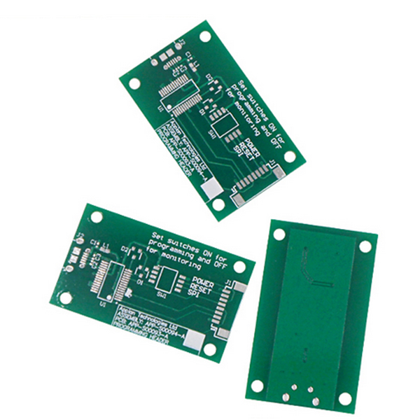
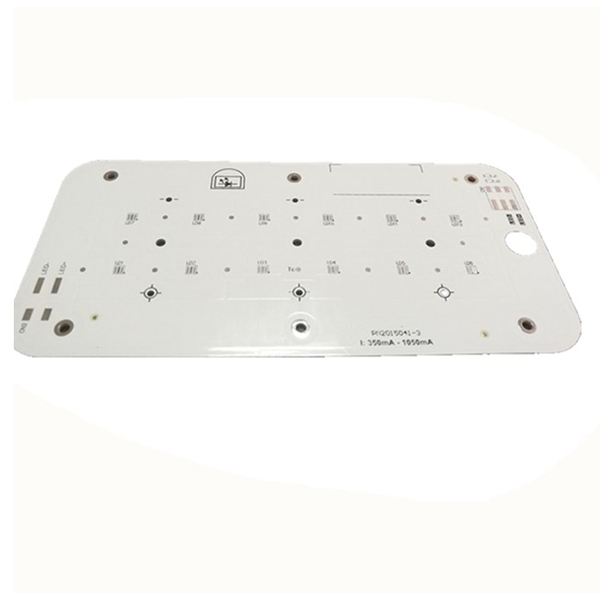
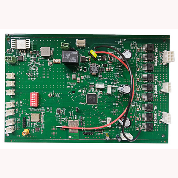
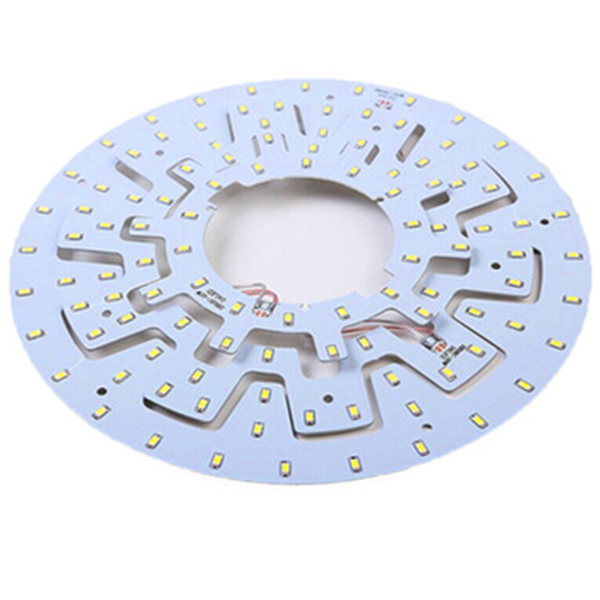
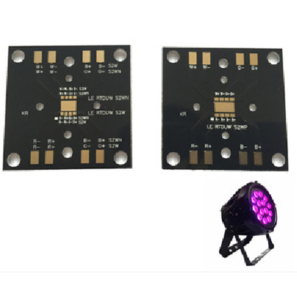
Product detail pictures:
Related Product Guide:
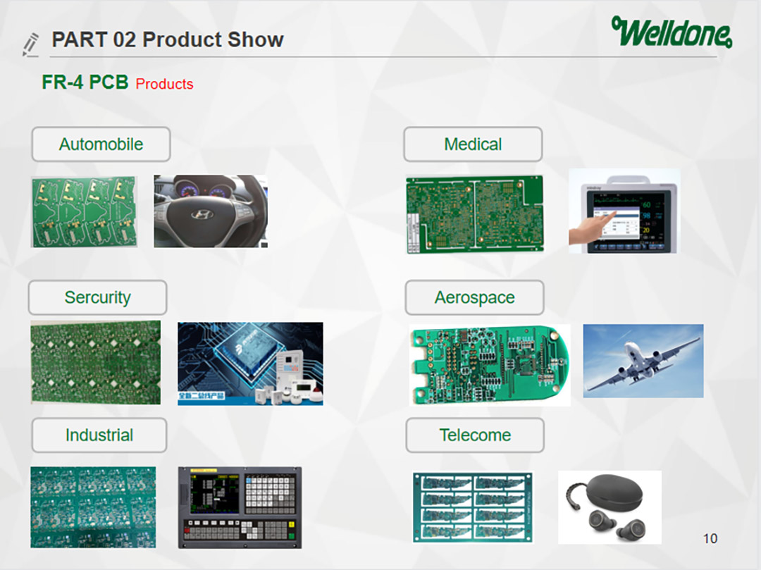
Gaining customer satisfaction is our company's aim forever. We will make great efforts to develop new and top-quality products, meet your special requirements and provide you with pre-sale, on-sale and after-sale services for OEM Customized Double Layer Pcb Design - EMC Design Spark FR4 PCB And The Printed Circuit Board – Welldone , The product will supply to all over the world, such as: Kenya, India, Kuwait, Due to our strict pursues in quality, and after-sale service, our product gets more and more popular around the world. Many clients came to visit our factory and place orders. And there are also many foreign friends who came for sight seeing, or entrust us to buy other stuff for them. You are most welcome to come to China, to our city and to our factory!
The sales manager has a good English level and skilled professional knowledge, we have a good communication. He is a warm and cheerful man, we have a pleasant cooperation and we became very good friends in private.
-
China Gold Supplier for Prototype Breadboard Pc...
-
Wholesale Price China Flexible Pcb Diy - High ...
-
Hot New Products Flexible Aluminum Pcb - Best ...
-
Discountable price Lighting Pcb For Car - Best...
-
Wholesale Discount Copper Core Pcb - RGB stage...
-

PriceList for 3d Printed Pcb - 3D fold able MC...