One of Hottest for Pcb Mechanical Design - EMC Design Spark FR4 PCB And The Printed Circuit Board – Welldone
One of Hottest for Pcb Mechanical Design - EMC Design Spark FR4 PCB And The Printed Circuit Board – Welldone Detail:
Product Details
Base Material:FR4
Copper Thickness:1oz
Board Thickness:1.6mm
Min. Hole Size:0.2mm
Min. Line Width:0.1mm
Min. Line Spacing:0.1mm
Surface Finishing:HASL
Solder Mask:Green
Silkscreen:White
PCB Test:Test-rig,Flying Probe Test
PCBA Test:X-ray,AOI Test,Functional test
Certificate:UL. ROHS. CE
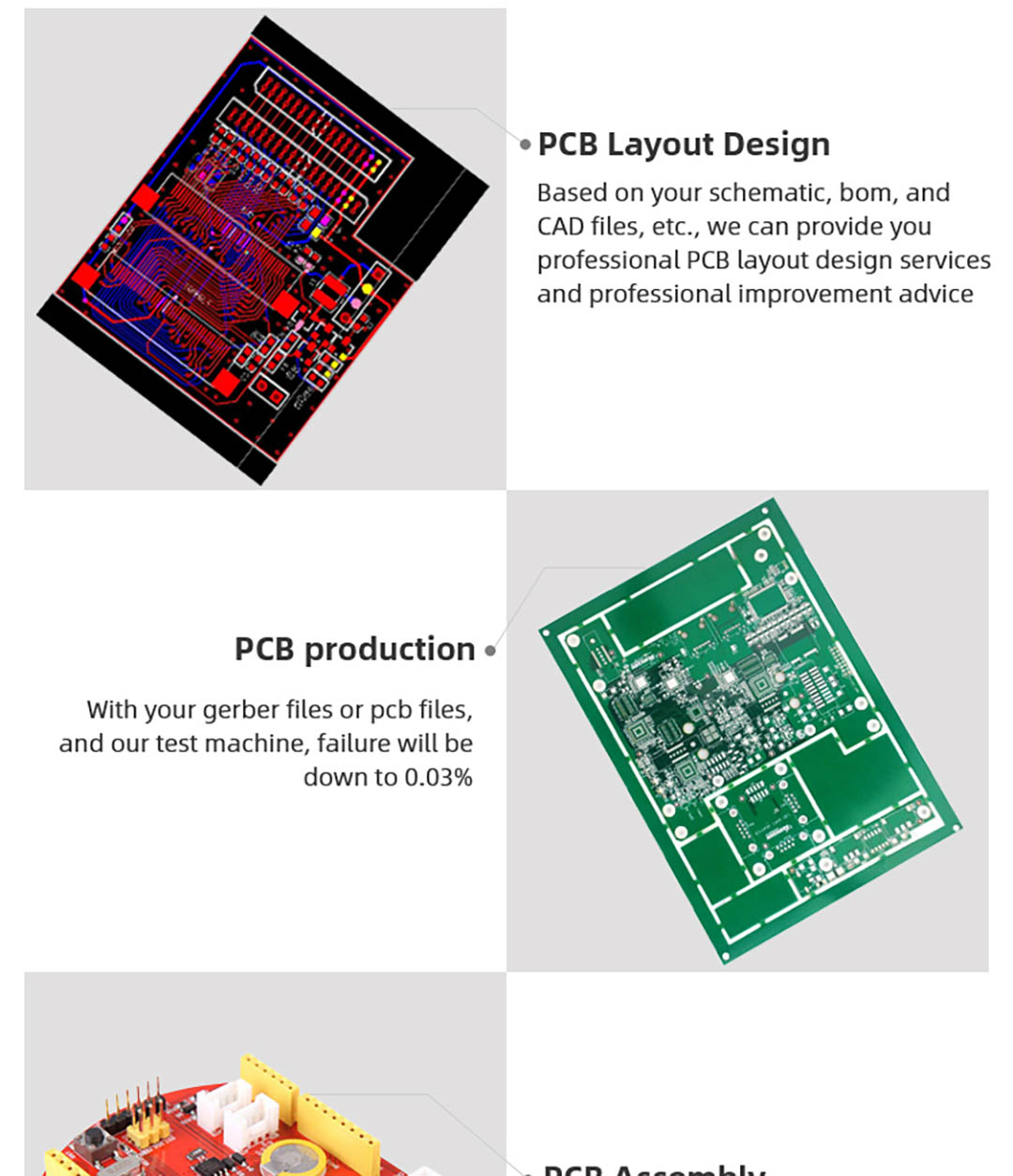
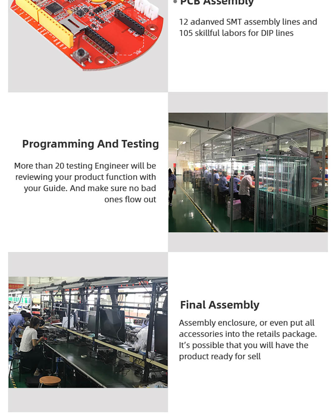
Type of services:High Quality PCB Manufacturing
Keywords:blank PCB board price
Service:One-stop Service
Layer:1-24layers
|
Item |
Specification |
|
|
1 |
Number of Layer |
1-18Layers |
|
2 |
Material |
FR-4,FR2.Ta-conic,Rogers, CEM-1 CEM-3,ceramic , crockery Metal-backed Laminate |
| 3 |
Surface Finish |
HASL(LF), Gold plating, Electrolysis nickel immersion gold, Immersion Tin, OSP |
|
4 |
Finish Board Thickness |
0.2mm-6.00 mm(8mil-126mil) |
|
5 |
Copper Thickness |
1/2 oz min;12 oz max |
|
6 |
Solder Mask |
Green/Black/White/Red/Blue/Yellow |
|
7 |
Min.Trace Width & Line Spacing |
0.075mm/0.1mm(3mil/4mil) |
|
8 |
Min.Hole Diameter for CNC Drilling |
0.1mm(4mil) |
|
9 |
Min.Hole Diameter for punching |
0.9mm(35mil) |
|
10 |
Biggest panel size |
610mm*508mm |
|
11 |
Hole Position |
+/-0.075mm(3mil) CNC Drilling |
|
12 |
Conductor Width(W) |
0.05mm(2mil)or; +/-20% of original artwork |
|
13 |
Hole Diameter(H) |
PTH L:+/-0.075mm(3mil); NON-PTH L:+/-0.05mm(2mil) |
|
14 |
Outline Tolerance |
0.125mm(5mil) CNC Routing; +/-0.15mm(6mil) by Punching |
|
15 |
Warp & Twist |
0.70% |
|
16 |
Insulation Resistance |
10Kohm-20Mohm |
|
17 |
Conductivity |
<50ohm |
|
18 |
Test Voltage |
10-300V |
|
19 |
Panel Size |
110×100mm(min);660×600mm(max) |
|
20 |
Layer-layer ministration |
4 layers:0.15mm(6mil)max; 6 layers:0.25mm(10mil)max |
|
21 |
Min.spacing between hole edge to circuity pattern of an inner layer |
0.25mm(10mil) |
|
22 |
Min.spacing between board outline circuitry pattern of an inner layer |
0.25mm(10mil) |
|
23 |
Board thickness tolerance |
4 layers:+/-0.13mm(5mil); 6 layers:+/-0.15mm(6mil) |
|
24 |
Impedance Control |
+/-10% |
|
25 |
Different Impedance |
+-/10% |
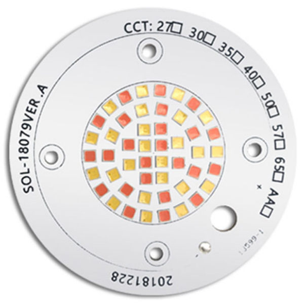
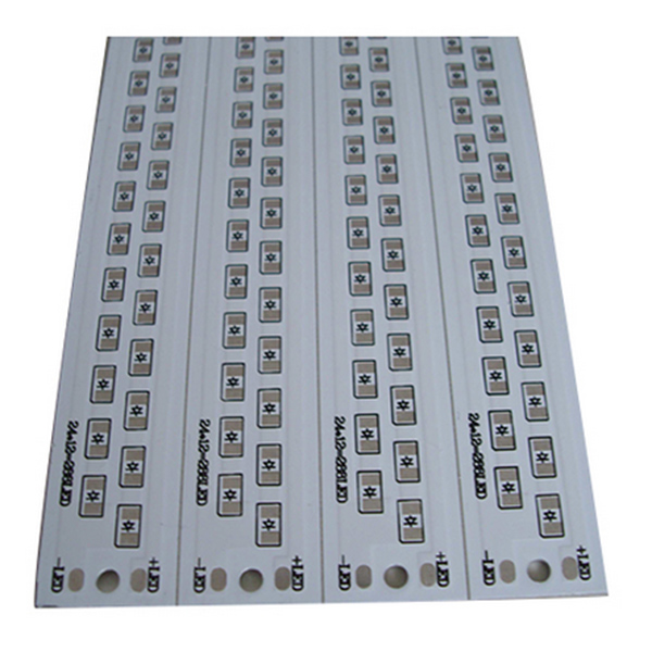
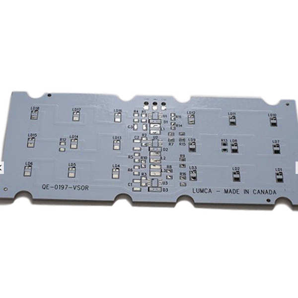
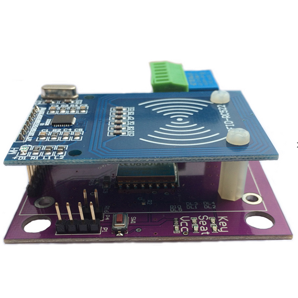
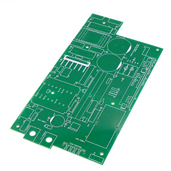
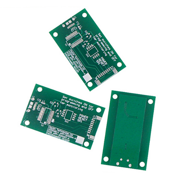
Product detail pictures:
Related Product Guide:
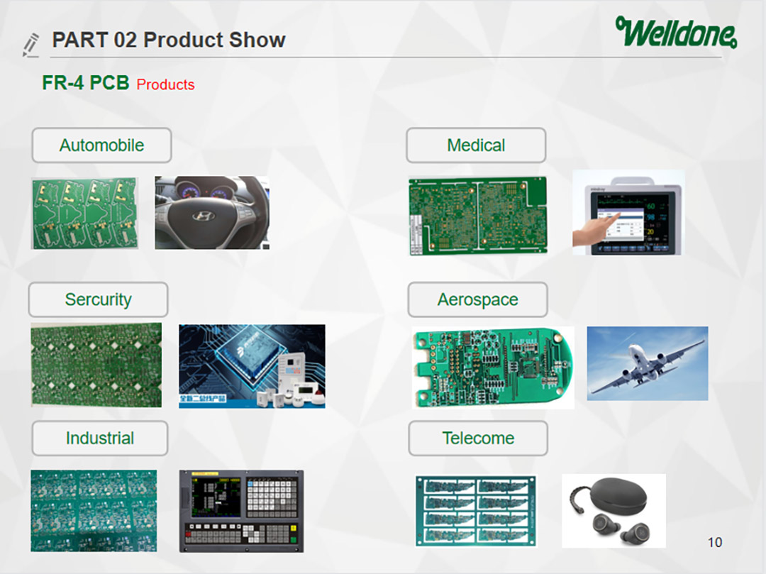
We've one of the most advanced generation tools, experienced and qualified engineers and workers, recognized good quality manage systems and a friendly skilled product sales workforce pre/after-sales support for One of Hottest for Pcb Mechanical Design - EMC Design Spark FR4 PCB And The Printed Circuit Board – Welldone , The product will supply to all over the world, such as: Philippines, Southampton, Swedish, Our company has always insisted on the business principle of "Quality, Honest, and Customer First" by which we have won the trust of clients both from at home and abroad. If you are interested in our solutions, you should do not hesitate to contact us for further information.
Although we are a small company, we are also respected. Reliable quality, sincere service and good credit, we are honored to be able to work with you!